Ceva Unveils Four NeuPro NPUs, Adds NeuPro Ultra for Data Centers
Ceva claims up to 2X AI throughput per mm² and 50% better energy efficiency than its first NeuPro generation. NeuPro Ultra moves the licensable NPU into data centers; general availability is planned for Q2 2027.
2 min readAI-assisted

Ceva's release artwork for the next-generation NeuPro NPU portfolio; it is an illustrative graphic, not a photo of the chips.
Image: Ceva
Source · Press image from the Ceva newsroom, used for news reporting.
Ceva, a licensor of chip design IP, said on Oct. 28 it has unveiled its next-generation NeuPro NPU portfolio, with up to 2X higher AI throughput per mm² and a 50% improvement in energy efficiency against the first generation. Both figures are Ceva's own claims, and the company gave no absolute throughput, TOPS or power number.
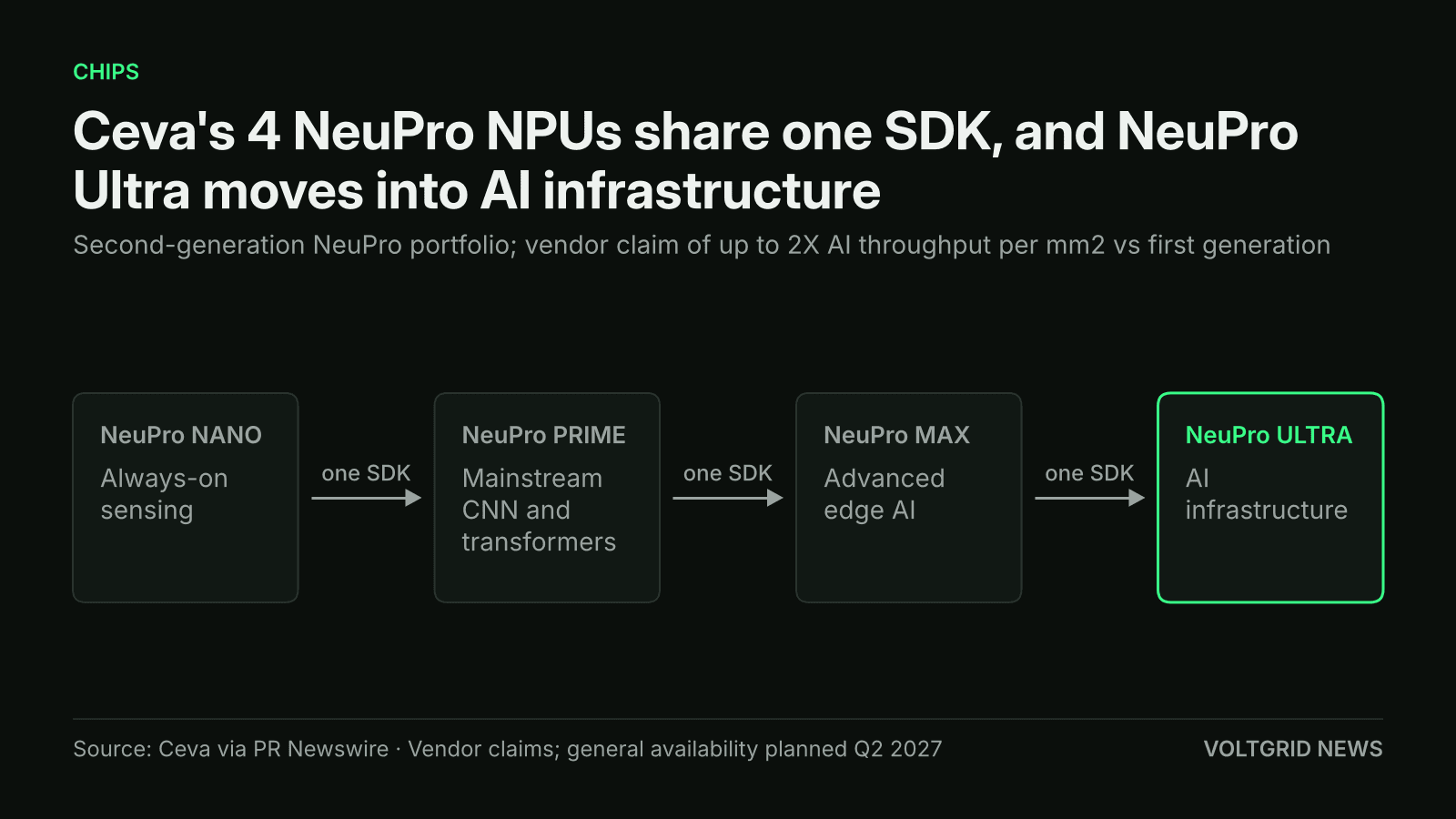
Ceva's four NPUs share one SDK, and NeuPro Ultra is the one aimed at AI infrastructure, according to the company.
Illustration (AI-generated)
The portfolio has four neural processing units (NPUs) on one architecture and one software development kit. NeuPro Nano targets always-on sensing, NeuPro Prime mainstream CNN and transformer workloads, and NeuPro Max advanced edge AI such as robotics and on-device assistants. The fourth, NeuPro Ultra, is for AI infrastructure.
Ceva sells licences, not chips. Customers who license the cores build their own silicon, so any effect on data center power or capacity depends on which of them tapes out a part and when. The company says more than 15 customers have licensed the first generation, and that leading semiconductor and system companies are evaluating the new cores. It names none for NeuPro Ultra.
What NeuPro Ultra is meant to do
Ceva says NeuPro Ultra supports large language model inference in cloud and data centers, with multi-core processing, multi-user operation and high memory bandwidth. It can also sit inside memory and connectivity silicon, applying neural processing to data movement rather than to the model, which Ceva says reduces unnecessary transfers. Ceva frames the shared constraint as power: microwatts and square millimetres at the sensor, megawatts and memory bandwidth in the data center.
The architecture adds FP4 and FP8 mixed-precision numerics, paged KV cache and dynamic shapes for longer contexts, and support for Mixture-of-Experts and linear attention models, plus pre-quantized checkpoints that need no separate calibration step. Ceva cites ABI Research's forecast that cloud AI inference capacity will grow at a 42% compound annual rate through 2035.
Custom inference silicon is already reaching clouds from other directions: Oracle plans to offer Cerebras and SambaNova chips, Reuters reported, as Voltgrid covered. Ceva is aiming at the layer below, the NPU block that chip designers can drop into their own parts.
What per-area throughput means for an NPU core
Ceva licenses NPU designs that chipmakers place on their own silicon, so the useful yardstick is how much work a core does for the die area and power it costs. That is why both of Ceva's headline figures are per square millimetre and per unit of energy, measured against its own first generation rather than as absolute speeds.
The FP4 and FP8 support matters for the same reason. Lower-precision numbers are smaller, so a core moves less data per operation, and Ceva says this cuts memory and data-movement demands. In data centers, that data movement, measured in memory bandwidth and megawatts, is the cost NeuPro Ultra targets, though no licensee has yet announced a chip using it.
What is not confirmed yet
The architecture is available now to select early-access customers, with general availability planned for the second quarter of 2027. Ceva has not published a process node, core count, clock speed or area for any of the four cores, and none of the performance figures has been independently measured. It will discuss the portfolio at technology symposiums in Hsinchu, Taiwan, on Nov. 2 and in Shanghai on Nov. 5.