SK hynix to Stretch 6F2 DRAM With EUV Before 4F2 or 3D DRAM
SK hynix said on its Oct. 28 earnings call it will scale 6F2 DRAM with EUV before moving to 4F2 or 3D DRAM, giving no dates. DigiTimes reports CXMT is pursuing 4F2.
2 min readAI-assisted
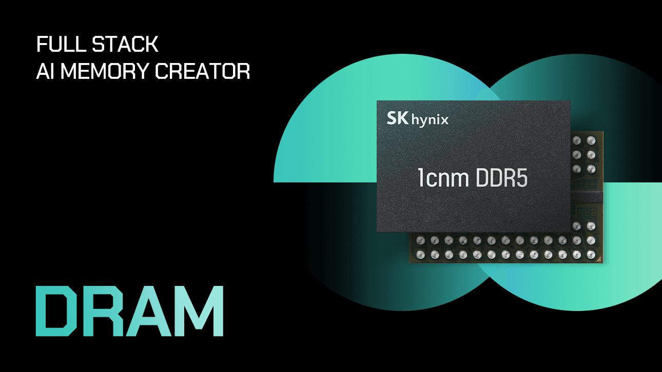
SK hynix promotional image of a DRAM chip; it does not show the 6F² or 4F² cell structure discussed on the call.
Image: SK hynix
Source · Press image from the SK hynix newsroom, used for news reporting.
SK hynix said on its Oct. 28 third-quarter earnings call that it will keep scaling its current 6F² DRAM cell with extreme ultraviolet (EUV) lithography and process work before it moves to the smaller 4F² cell or to 3D DRAM, according to the call transcript published by The Motley Fool.
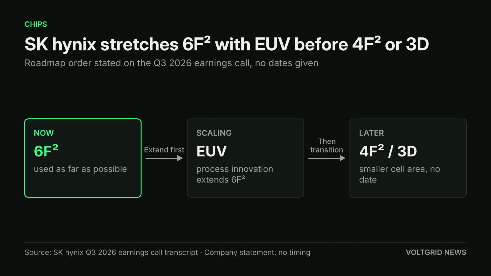
SK hynix said it will extend 6F² with EUV scaling before moving to 4F² or 3D DRAM, and gave no dates, according to the Q3 2026 earnings call transcript.
Illustration (AI-generated)
An analyst from Mirae Asset Securities asked what SK hynix is doing to prepare for 4F², given that other memory makers are working on new cell structures. An SK hynix executive answered that 4F² is a next-generation technology with a smaller cell area than 6F², and that whether and when it applies depends on each company's scaling capability, process environment and cost structure. The company said it has secured the ability to expand the 6F² platform further through EUV-based scaling and process innovation. The DigiTimes headline links the remarks to CXMT's push toward 4F²; Voltgrid read only the headline of that paywalled report.
Why SK hynix is staying on 6F² for now
The executive called the proven platform the most efficient route: its mass-production reliability and cost competitiveness are already established. A new cell structure needs yield, reliability and cost competitiveness, plus finished product design and customer qualification, the executive said. For that reason, the timing of technology development and the timing of commercialization are separate.
The choice matters for supply. SK hynix said it expects DRAM bit shipments to grow in the mid-20% range quarter on quarter in the fourth quarter, as 1c-nanometer output rises and the M15X fab ramps for HBM4. Management also said memory supply cannot keep pace with demand and that the constraint is projected to continue through 2030.
Voltgrid News reported that Micron has also ruled out a CXMT-style 4F² design and is staying with 6F² and 3D DRAM. SK hynix and Micron have both said they will stay on 6F² for now: Micron has ruled out a CXMT-style 4F² design, while SK hynix keeps 4F² and 3D DRAM on its road map. On the earnings themselves, see SK hynix's Q3 profit of 83.3 trillion won.
What 6F² and 4F² Mean for DRAM
A DRAM cell stores one bit, and its footprint is quoted in multiples of F², the square of the smallest feature a chipmaker can print. An SK hynix executive said 4F² has a smaller cell area than 6F², the layout SK hynix uses now. The Motley Fool's glossary for the call transcript describes 4F² as meant to raise density beyond 6F² limits.
A smaller cell fits more bits on a wafer, but SK hynix said a new cell must also reach yield, reliability and cost targets and pass customer qualification. With supply unable to keep pace with demand through 2030, in the company's view, it is adding output from the 6F² layout it already mass-produces.
What is not confirmed yet
SK hynix gave no date for 4F² or 3D DRAM, no EUV layer count for its DRAM and no cost or density figure. It described a step-by-step road map that runs from extreme scaling of existing DRAM to 4F² and 3D DRAM, and said each technology will be applied to the right product when it is ready technologically and economically. The transcript marks the answers as interpreted from Korean and does not name the executive who gave them. CXMT's own 4F² product claims have not been verified by Voltgrid.