Samsung 2nm Project Orders to More Than Double, Major Volume in 2H 2027
Samsung says 2nm project orders will more than double in 2026, but major-customer production starts in 2H 2027. No hyperscaler is named; 4nm HBM base dies drove Q3's foundry gain.
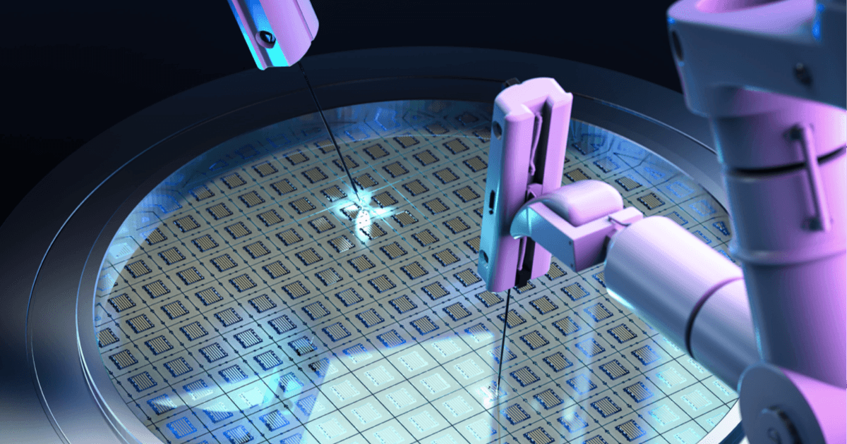
Samsung Foundry's own illustration of wafer testing; it is not a photo of a specific 2nm line or fab.
Image: Samsung Foundry
Source · Press image from the Samsung Foundry website, used for news reporting.
Samsung Electronics told investors on Oct. 29 that its foundry's 2nm project orders will more than double in 2026 from 2025, yet mass production for its major 2nm customers will not begin until the second half of 2027. On the call, the foundry executive credited 4nm base dies for high-bandwidth memory (HBM) for the quarter's revenue gain, while 2nm still has to prove itself in volume.
That matters beyond Samsung. Its rival TSMC already draws 8% of its wafer revenue from 2nm, and Samsung says hyperscalers are among its 2nm order wins but has named none, with volume for its major 2nm customers not due until the second half of 2027.
What Samsung Said on the Q3 Call
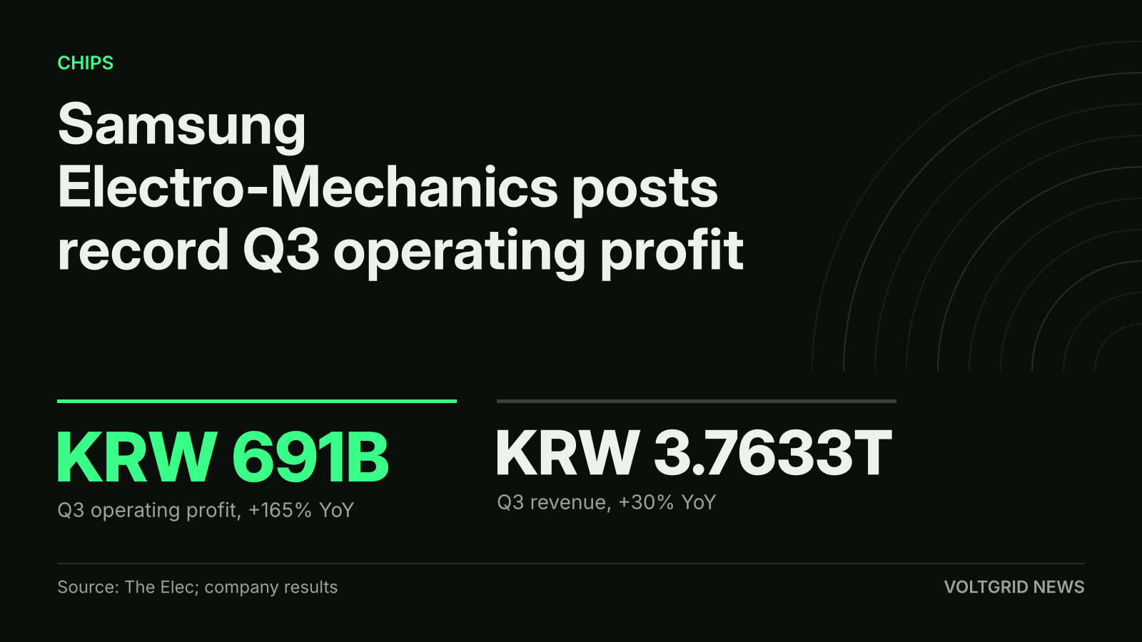
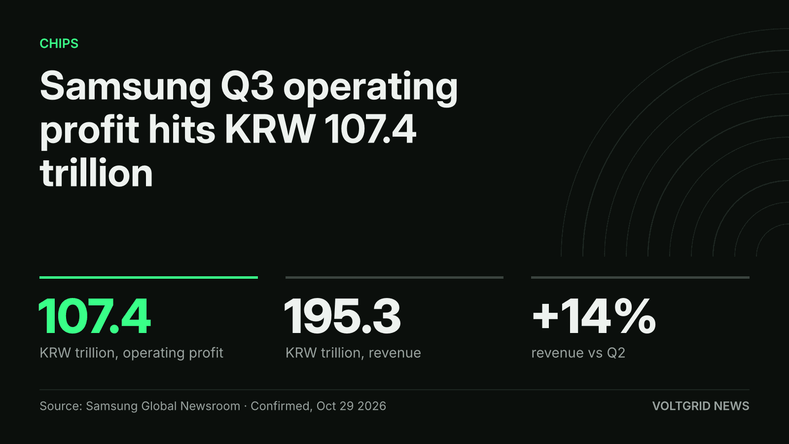
In its results release, Samsung said the Foundry Business improved revenue and earnings markedly in the third quarter. It credited growth in HBM base-die sales, higher advanced-node sales and continued 2nm order wins centred on high-performance computing (HPC) customers, including major hyperscalers. It named none of them. On the call, the foundry executive said the quarter-on-quarter revenue gain came from 4nm HBM base dies. Samsung does not report foundry revenue or profit on its own; the Device Solutions division as a whole posted KRW 106.5 trillion of operating profit on KRW 147.1 trillion of revenue, a result Voltgrid covered on the day.
For the fourth quarter, the release says the Foundry Business plans to achieve double-digit revenue growth from new mobile products, a mass-production ramp of 4nm NPUs and more memory-related sales. The call transcript describes the 4nm item as full-scale MPU production for a major customer; this article uses the release's wording. On the call, Samsung also said mass production of new mobile products on its second-generation 2nm process starts this quarter, and that new products for its major 2nm customers enter mass production in the second half of 2027.
Samsung added that it projects demand on nodes below 8nm to substantially exceed capacity, with utilization above 100%, per the call. It expects HPC to rise above 50% of its foundry sales mix. On 1.4nm, the node after 2nm, Samsung said it is in talks with multiple customers and that plans are final for test-chip development with one of them. Seoul Economic Daily, in an AI-translated report, rendered the same answer as chip development already confirmed with some clients. The transcript is the narrower reading, and no customer or date was given.
Why HBM Base Dies Count as Foundry Revenue
An HBM stack is layers of DRAM sitting on a logic die, the base die, which connects the stack to the processor. HBM4 doubled that connection to 2,048 I/O pins per stack, Samsung says, and its HBM4 uses a 4 nm logic base die made by its own foundry. Samsung's results release then lists base-die sales growth under the Foundry Business.
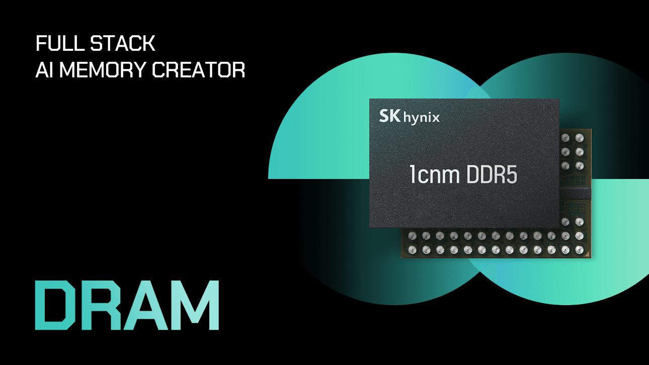
The base die is also contested: SK hynix showed its 16-layer HBM4 with a base die made in TSMC's advanced logic process. For Samsung, memory demand therefore adds foundry orders, but it has not split out foundry revenue, so the size of that lift next to its 2nm orders cannot be measured from the filing.
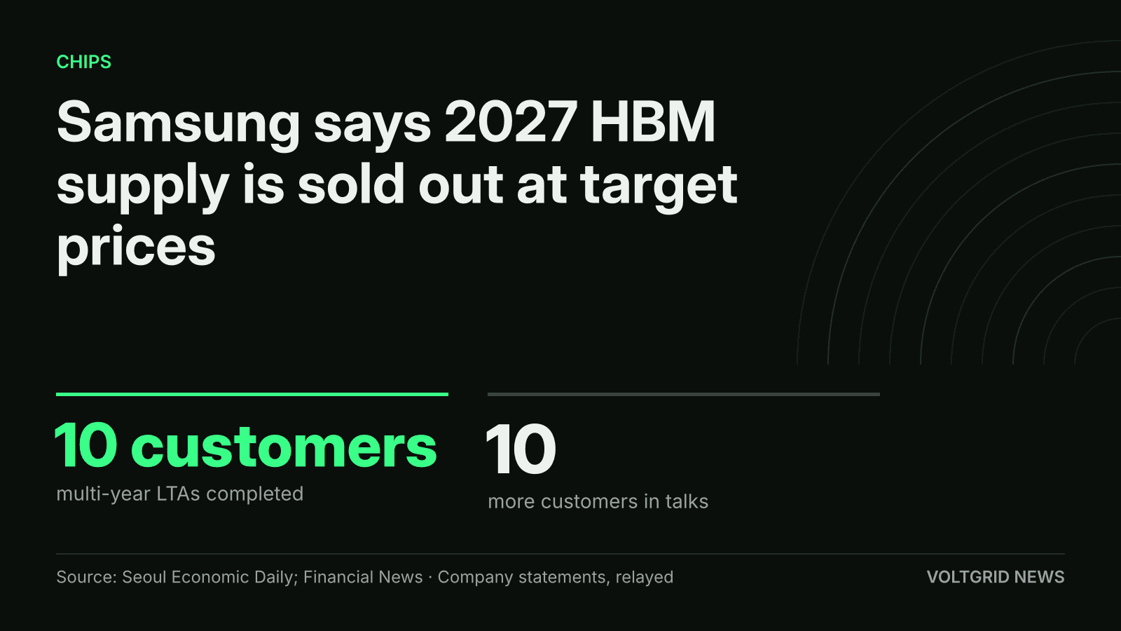
Samsung's foundry makes its HBM4 base dies on 4nm, and its results release reports base-die sales growth under the Foundry Business. Samsung said on its call, per Korean press, that planned 2027 HBM supply is sold out at target prices; Voltgrid reads that as secure internal demand for 4nm base dies.
The 2nm story rests on orders, not shipments. Samsung did not say what a project order counts or give a 2025 base, so the doubling cannot be turned into designs or wafers, and it said it is still working on yield stabilization for 2nm without giving a figure. The first external proof point it named is the second half of 2027, the same year it expects its fab in Taylor, Texas, to start operating. On the call, Samsung said Taylor Fab 1 has begun clean-room operations, equipment installation has started and wafers are going in for line setup, which fits the tool orders reported for the site.
The nearer test is the Q4 mobile ramp. Samsung did not name the product. System LSI said only that the Exynos 2700 has better AI and gaming performance and that its development and production are on schedule. Seoul Economic Daily reported that the Exynos 2700 is made on Samsung's 2nm process and that Samsung is reportedly working to use it in the Galaxy S27 series, which is also expected to use Qualcomm's Snapdragon 8 Elite Gen 6. That the Q4 2nm products are the Exynos 2700 is Voltgrid's inference, not Samsung's statement. If it holds, the first high-volume second-generation 2nm chip is Samsung's own, and its battery life and sustained performance in independent reviews will be the first public read on the node.
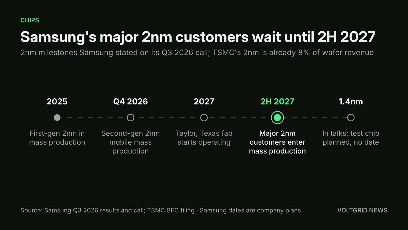
Samsung's 2nm volume for major customers is scheduled for 2H 2027, while TSMC's 2nm already makes up 8% of its wafer revenue.
Illustration (AI-generated)
Counter-Argument: Capacity Is the Constraint
The strongest counter-argument is capacity. A foundry that says its sub-8nm lines will run above 100% utilization is short of supply, not of customers. Samsung raised Q3 capital expenditure to KRW 29 trillion, KRW 27.2 trillion of it in Device Solutions, and expects about KRW 84.4 trillion for 2026 with KRW 76.8 trillion in that division, aimed in part at new fabs for AI and HPC demand. The release also says System LSI's custom SoC business signed new customer partnerships. On that reading, the hyperscaler 2nm wins are real commitments waiting for Taylor, and 2H 2027 is a fab schedule rather than a sign of weak 2nm demand.
That case is fair, but it remains unproven. Samsung has not named one 2nm hyperscaler customer, has not disclosed a yield, and splits out no foundry profit, so none of the claims can yet be checked against results.
What it means for TSMC and chip buyers
TSMC's third-quarter filing shows how far ahead the incumbent is. Its 2nm made up 8% of third-quarter wafer revenue and 3nm 33%, and it guided fourth-quarter revenue to US$52.3 billion to US$54.3 billion, citing a steep 2nm ramp. TSMC began high-volume 2nm manufacturing in the fourth quarter of 2025 and expects its N2-family capacity to more than double in 2027. For hyperscalers designing custom accelerators, Samsung's 2nm is a possible hedge on TSMC capacity and pricing, but Samsung schedules volume for its major 2nm customers only for the second half of 2027.
What to Watch Through 2H 2027
The first marker is Q4 2026: whether Samsung's foundry posts the double-digit growth it promised and which phones carry second-generation 2nm silicon. Next comes the Galaxy S27 launch, expected early next year, and the first independent measurements of the Exynos 2700. The deciding date is the second half of 2027, when Samsung says production for its major 2nm customers and operations in Taylor begin. A named 1.4nm customer, or a test-chip result, would show whether the node after 2nm is drawing real designs.
Sources
- 01Samsung Electronics Announces Third Quarter 2026 ResultsSamsung Newsroom · news.samsung.com
- 02Earnings call transcript: Samsung Electronics posts record Q3 2026 profitInvesting.com · za.investing.com
- 03TSMC Reports Third Quarter EPS (Form 6-K)TSMC (SEC Form 6-K) · sec.gov
- 04Samsung Electronics Says It Is in Talks With Multiple Clients on 1.4-Nanometer Foundry ProcessSeoul Economic Daily · en.sedaily.com