Samsung Reportedly Plans 25 Trillion Won 2nm/4nm Fab at Giheung
Samsung is reportedly building a 2nm and 4nm foundry fab at Giheung, estimated at 25 trillion won, to add HBM4 base-die capacity and prepare 2nm HBM5 dies. Samsung has not confirmed.
Chips & Power DeskEdited by Ege Erten
2 min readAI-assisted
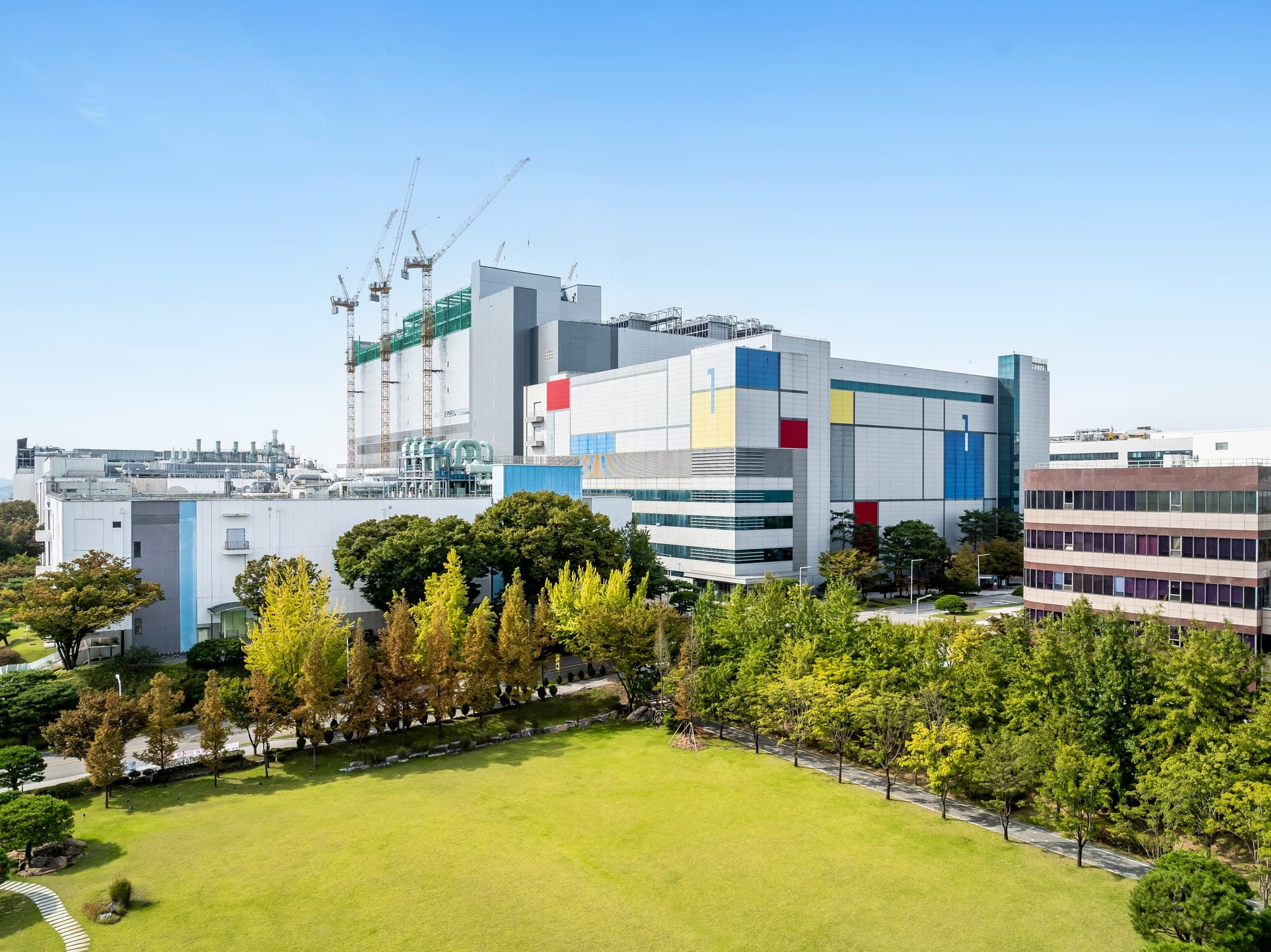
Samsung's Giheung campus in an official newsroom photo. The image predates the reported Kairos plan and does not show the new fab site.
Image: Samsung Electronics
Source · Press image from the Samsung Newsroom, used for news reporting. · License
Samsung Electronics has decided to build a 2-nanometer and 4-nanometer class foundry fab at its Giheung campus in Yongin, South Korea, with the Kairos project estimated at about 25 trillion won ($19.23 billion), Seoul Economic Daily and BusinessKorea reported on Nov. 4, 2026.
The reports cite industry sources; Samsung has not confirmed the plan. The fab will go up on the site of the Samsung Advanced Institute of Technology building (SR5) and the engineering college building (CDI), both demolished last month. The complex will have a main building, a green building and a substation, with Samsung E&A handling engineering, procurement and construction. Financial News reported separately on Nov. 4 that Samsung E&A is already carrying out structural work on the site.
Why it matters: the driver is HBM (high-bandwidth memory). Samsung makes HBM4 core dies at its Hwaseong and Pyeongtaek campuses, but the 4nm base dies that sit under each stack come from only some lines at those sites, according to Seoul Economic Daily. A Giheung fab would let base-die capacity grow in step with core-die output. The industry expects Samsung's HBM supply, measured in bits, to grow 52% a year on average for three years through 2028, the paper said.
Cost and layout
Seoul Economic Daily puts the Kairos fab at about 25 trillion won. Samsung is understood to have drawn up purchase quotes for several dozen extreme ultraviolet (EUV) lithography machines worth 8 trillion to 10 trillion won. With cleanrooms and other process tools, the total is calculated to exceed 20 trillion won. Converting part of Line 6, an 8-inch (200 mm) line that makes image sensors, display driver chips and power chips, into an advanced packaging facility could lift the figure to 30 trillion won, observers told the paper. BusinessKorea converted the same figures to $19.23 billion, more than $15.38 billion and $23.08 billion.
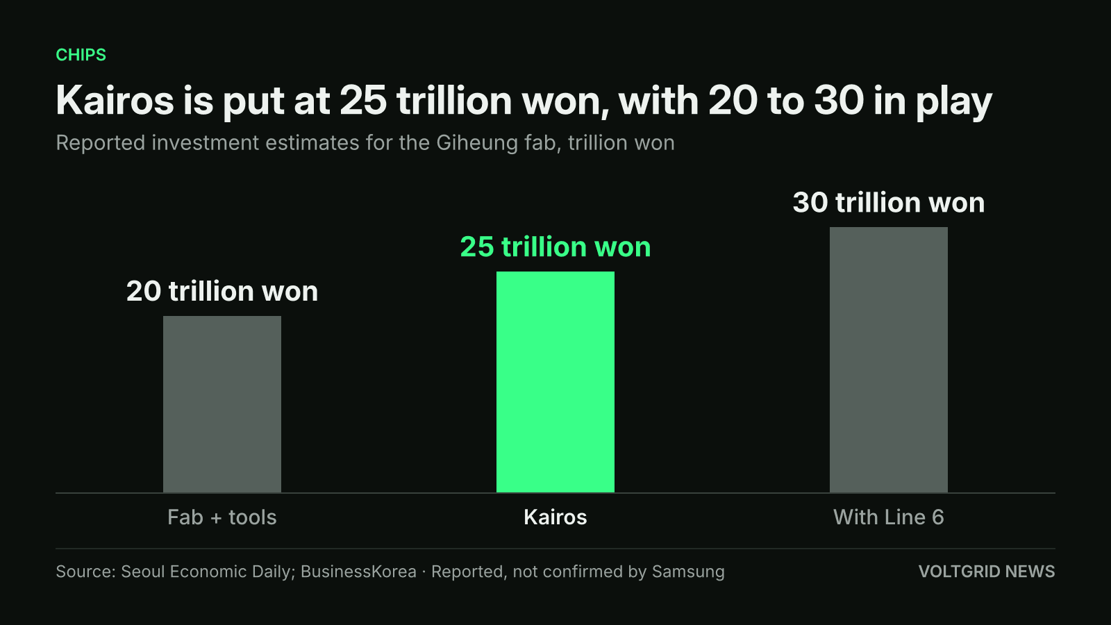
Reports put Kairos at 25 trillion won, with estimates running from 20 trillion won to 30 trillion won; Samsung has not confirmed any figure.
Illustration (AI-generated)
Like Samsung's new Pyeongtaek plant, the Kairos fab is planned in four production phases. The 2nm line is aimed at HBM5, whose base die is likely to move from 4nm to 2nm, according to both outlets. HBM4 and HBM4E base dies stay on 4nm. Financial News added that the fab is designed so it could later be converted to memory production, though that would need extra equipment and process changes. It said a DRAM line had also been considered before foundry was chosen.
Samsung's Recent HBM and Foundry Moves
The plan fits Samsung's recent moves. As Voltgrid reported on Oct. 20, it is restarting Pyeongtaek Fab 5 to win back HBM share from SK hynix, and it has reportedly ordered tools to lift Taylor Fab 1 to 20,000 2nm wafers a month.
What is not confirmed yet
Samsung has not announced Kairos, its cost, the node split between 2nm and 4nm, wafer capacity or a start date for production. The 25 trillion won and 30 trillion won figures are estimates from unnamed industry sources, and the EUV tool count is not given beyond "several dozen". The HBM5 timing is the papers' expectation, not a Samsung statement.