Samsung Reportedly to Make 2nm HBM Base Dies for AMD, NVIDIA at Taylor
Maeil Business reports Samsung's second Taylor fab has orders for its entire output, mostly AMD, for 2nm HBM base dies from 2030. Samsung declined to comment and has confirmed no customer.
Chips & Power DeskEdited by Ege Erten
3 min readAI-assisted
Follows our story: Samsung Reportedly Orders Tools to Lift Taylor Fab 1 to 20,000 2nm Wafers
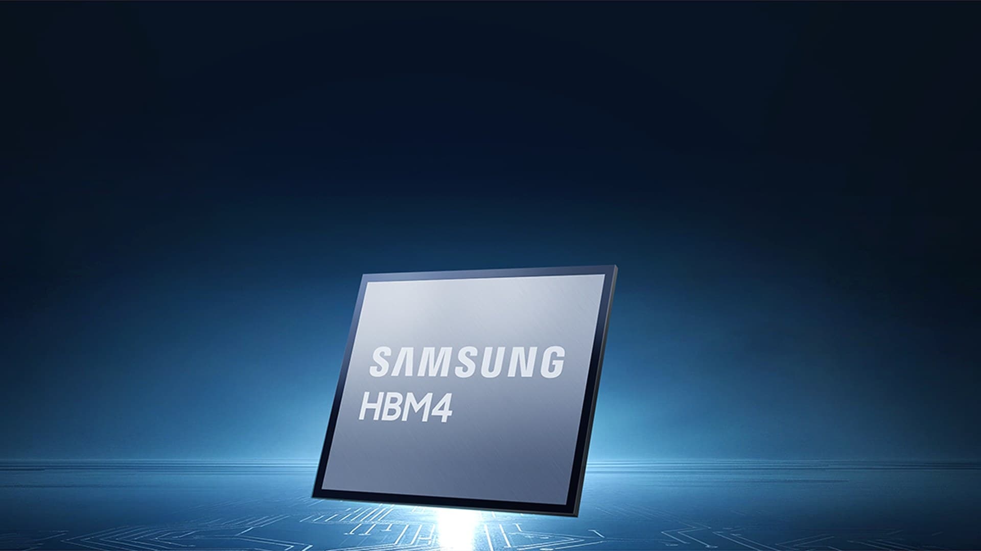
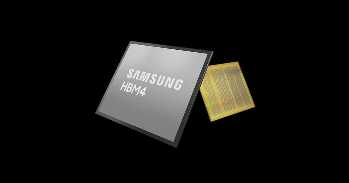
Samsung's HBM4 (Samsung product image). The Taylor base dies in the report are not pictured.
Image: Samsung Semiconductor
Source · Product image from Samsung Semiconductor's HBM4 page, used for news reporting.
Samsung Electronics will reportedly make HBM base dies for AMD and NVIDIA on 2nm at its second Taylor, Texas, fab, with mass production in 2030, Maeil Business Newspaper reported on Nov. 3.
Reuters, relaying the Maeil report, said the paper cited industry sources. The plant has orders for its entire output, and most of that volume is for AMD, according to Maeil. It will cover about 2.7 million square feet, roughly 1.5 times the first Taylor fab, which has a contract with Tesla. Construction is due to start formally this month, according to Maeil, with equipment installed from February 2029. Samsung declined to comment, so none of this is confirmed by the company.
The report extends our coverage of the site. As Voltgrid reported on Oct. 23, ZDNet Korea said Samsung had ordered tools to lift Taylor Fab 1 to 20,000 2nm wafers a month, and that a second fab was planned for operation in 2030. Maeil now gives that second building a product and customers: the logic layer that sits at the bottom of an HBM stack and controls how the memory talks to the processor.
What Samsung has said about Taylor Fab 2
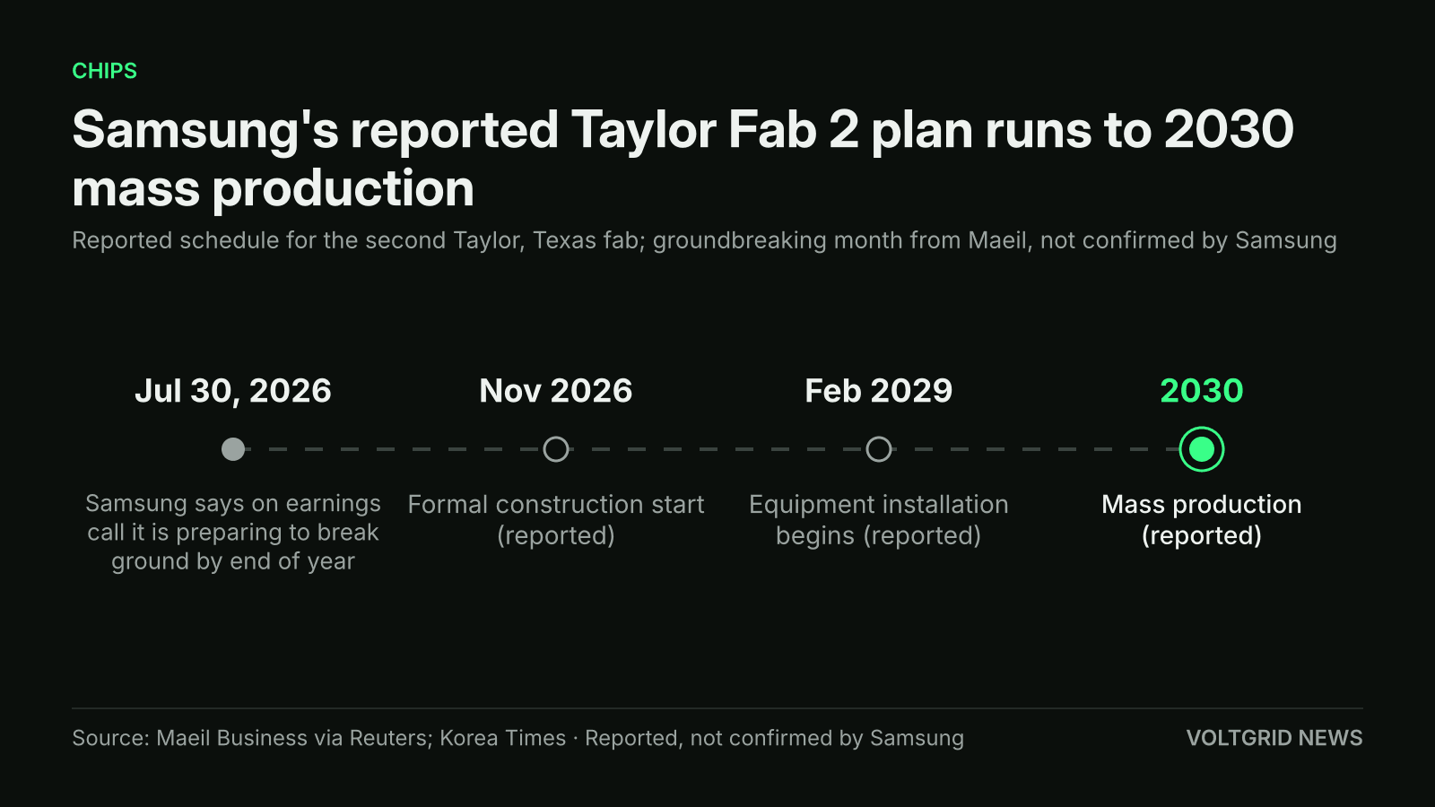
Maeil reports construction starts in November 2026, equipment arrives from February 2029 and mass production begins in 2030; Samsung has not confirmed the dates.
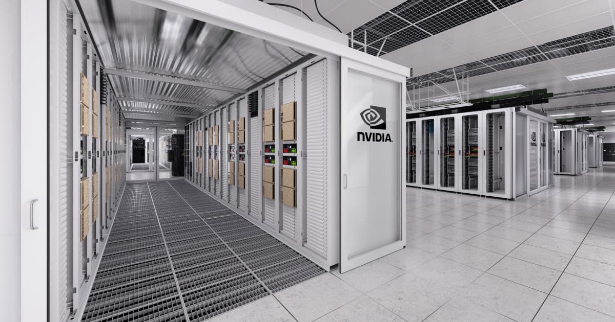
Illustration (AI-generated)
Samsung itself has said less. On its second-quarter earnings call on July 30, it told investors it was preparing to break ground on a second Taylor fab by the end of this year, targeting mass production in 2030, the Korea Times reported. It said foundry revenue had improved on higher demand for HBM base dies and products from North American customers. It also said its advanced-process expansion was not keeping pace with demand and that it would gradually expand 2nm capacity. We found no Samsung statement naming AMD or NVIDIA as Taylor customers.
Reuters gives no figure for wafer capacity or investment, and Maeil's account does not say how many base dies the plant could turn out. The 2030 start also places the output well after the tightest years. On the same July call Samsung said it did not expect a significant rise in industry memory supply before 2028, and Korean press reported that Samsung said on its Oct. 29 call that its 2027 HBM supply is sold out. A Texas base-die line would not ease the next three years of allocation.
What an HBM Base Die Does
Every HBM stack sits on a base die, a logic chip under the DRAM layers that runs the connection to the processor. HBM4 doubles that connection from 1,024 to 2,048 pins per stack, Samsung says, and the base die drives all of them.
Because it is logic, not memory, a foundry can build it: Samsung says its HBM4 uses a 4nm base die under 1c DRAM. A 2nm base die, as Maeil reports for Taylor, would upgrade the logic layer, not the memory. On the reported schedule that output starts in 2030, while Samsung's Oct. 29 results release says Taylor operations begin in 2027.
Where the base die fits
Samsung currently builds the base die for its HBM4 on a 4nm process, and The Elec reported that moving its next modem to 2nm frees 4nm lines for HBM, as Voltgrid reported on Oct. 21. Samsung has not said where the DRAM core dies would be made or the stacks assembled for a Taylor base die, so the report does not settle where the finished HBM would be built.
What is not confirmed yet
Samsung has not confirmed the customers, the 2nm node, the order book or the November construction date. Our earlier report that NVIDIA had asked all three HBM makers to build base dies on TSMC 3nm does not obviously fit a Samsung 2nm base die for the same customers, and the Maeil report as relayed by Reuters does not address the difference. Watch for a groundbreaking announcement, a named customer and any statement of the node and wafer plan.