Qualcomm HBC Test Stack Tops 5x HBM4 Bandwidth per Watt, Short of 6x Goal
Qualcomm says a two-layer HBC sample delivered more than 5x HBM4's bandwidth per watt by its own comparison with HBM4's specifications, short of its 6x projection, ahead of AI250 sampling in 2027.
Chips & Power DeskEdited by Ege Erten
3 min readAI-assisted
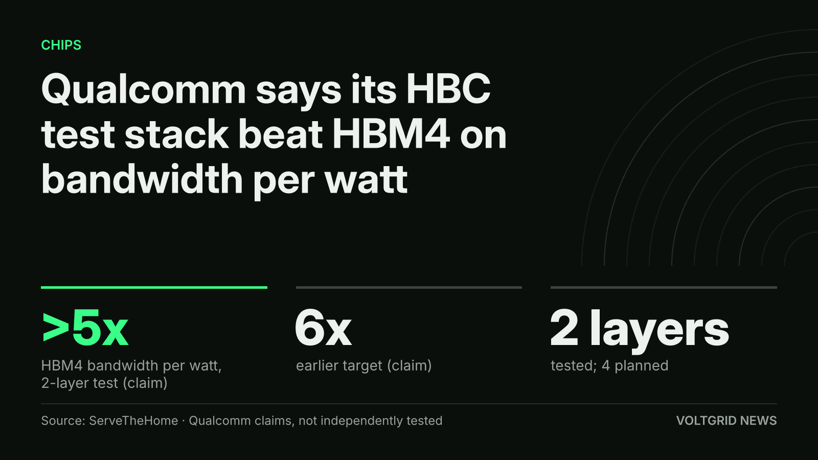
Qualcomm's claims for its HBC test stack: more than 5x HBM4 bandwidth per watt on 2 layers, against an earlier 6x target; 4 layers are planned.
Illustration (AI-generated)
Qualcomm said on Nov. 2 that it has completed initial validation of High Bandwidth Compute (HBC), its stacked-memory design for the Dragonfly AI250 accelerator, measuring more than 5x the bandwidth per watt of HBM4 on a two-layer test stack, according to ServeTheHome.
The test used an early sample in Qualcomm's San Diego labs, run on an automated tester as both an LPDDR5X device and an HBC device. Qualcomm told ServeTheHome the measured bandwidth was 18x that of external LPDDR5X, but it did not disclose absolute figures. The 5x efficiency result is Qualcomm's own, set against HBM4's specifications as ServeTheHome describes it, and it falls short of the 6x the company had projected.
The consequence is in the power budget. Data movement is a large share of an accelerator's energy use, and HBC places a small compute die at the base of a stack of LPDDR5X DRAM dies, so the most bandwidth-hungry operations happen next to the data. If the efficiency survives in a full product, the same rack power buys more memory traffic. Qualcomm's product page lists the AI250 at 133 TB/s of effective bandwidth per card and 140 kW per rack, a figure it labels thermal design power rather than measured draw.
What Bandwidth per Watt Does and Does Not Show
Bandwidth per watt asks how much data moves for each watt spent moving it. Qualcomm's 5x is a ratio, not a lab race: its own measurement of a two-layer HBC stack set against HBM4's published specifications, according to ServeTheHome. For scale, JEDEC's HBM4 standard allows up to 2 TB/s per stack over a 2,048-bit interface.
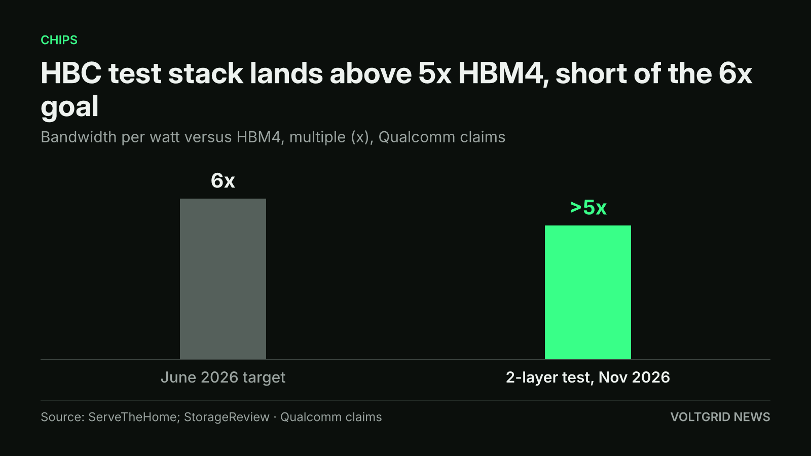
Qualcomm's claims: the 2-layer HBC test stack measured more than 5x HBM4 bandwidth per watt, below the earlier 6x target.
Illustration (AI-generated)
The 18x is a separate comparison, against external LPDDR5X, and Qualcomm gave no absolute figure. The AI250's 133 TB/s is an effective figure per card, so it cannot sit beside an HBM stack's TB/s. Until stack-level numbers appear, the result shows direction rather than a verified margin over HBM4, and 5x trails the 6x Qualcomm projected.
What was and was not tested
The stack had two DRAM layers. Shipping parts are planned with four, so full-height stacks have not been measured. Qualcomm said the validation also covered thermal behavior but gave no numbers, and heat is a known risk when an active compute die sits at the base of a memory stack.
HBC differs from HBM in packaging. Jon Peddie Research describes it as LPDDR stacked on a logic die through dense through-silicon vias and mounted on a standard 2D organic substrate, which avoids the 2.5D interposer packaging, such as CoWoS, that HBM needs and that has limited supply. Memory bonding with TSVs is still required, so the hard manufacturing step shrinks rather than disappears.
Timeline and context
According to Qualcomm, via ServeTheHome, the AI250 will begin sampling in the first half of 2027. Qualcomm's June investor roadmap, as covered by StorageReview, put commercial sampling of HBC Gen 1 with the AI250 in mid-2027, and Jon Peddie Research reports first-generation commercialization in fiscal 2027. Qualcomm also plans HBC Gen 2 for the later AI300.
For Qualcomm the memory work carries a larger bet. As Voltgrid reported, the company is cutting jobs from November as it pivots to AI chips, leaning on the AI200 and AI250 line. Memory architecture is also moving elsewhere: Groq was reportedly weighing 3D-stacked DRAM for its next chip, while NVIDIA's Rubin HBM4 sits at 19.2 TB/s in our earlier comparison with AMD's MI455X.
What is not confirmed yet
No independent party has tested the 5x or the 18x figures, and Qualcomm has not published the bandwidth numbers behind them. It is unclear how the result scales from two layers to four, what the thermal limits are, and which memory partners will build the stacks. The 133 TB/s card figure is what Qualcomm calls effective bandwidth, so it should not be set directly against HBM's per-stack numbers. The sampling window is also worded differently across Qualcomm's statements.
Sources
- 01Qualcomm pushes compute next to memoryJon Peddie Research · jonpeddie.com
- 02Qualcomm Validates HBC Stacked Memory Ahead of 2027 Dragonfly AI250 SamplingServeTheHome · servethehome.com
- 03Qualcomm Unveils Dragonfly Data Center Roadmap: C1000 CPU, AI300 Accelerator, and Modular AcquisitionStorageReview · storagereview.com