CoAsia Semi Ships Over-800 mm² Switch Chips on Samsung 4nm, $175M Project
CoAsia Semi said on Nov. 2 it began mass-production wafer shipments in mid-October of HPC switch chips on Samsung's 4nm process, in a $175 million project that runs to 2029.
Chips & Power DeskEdited by Ege Erten
2 min readAI-assisted
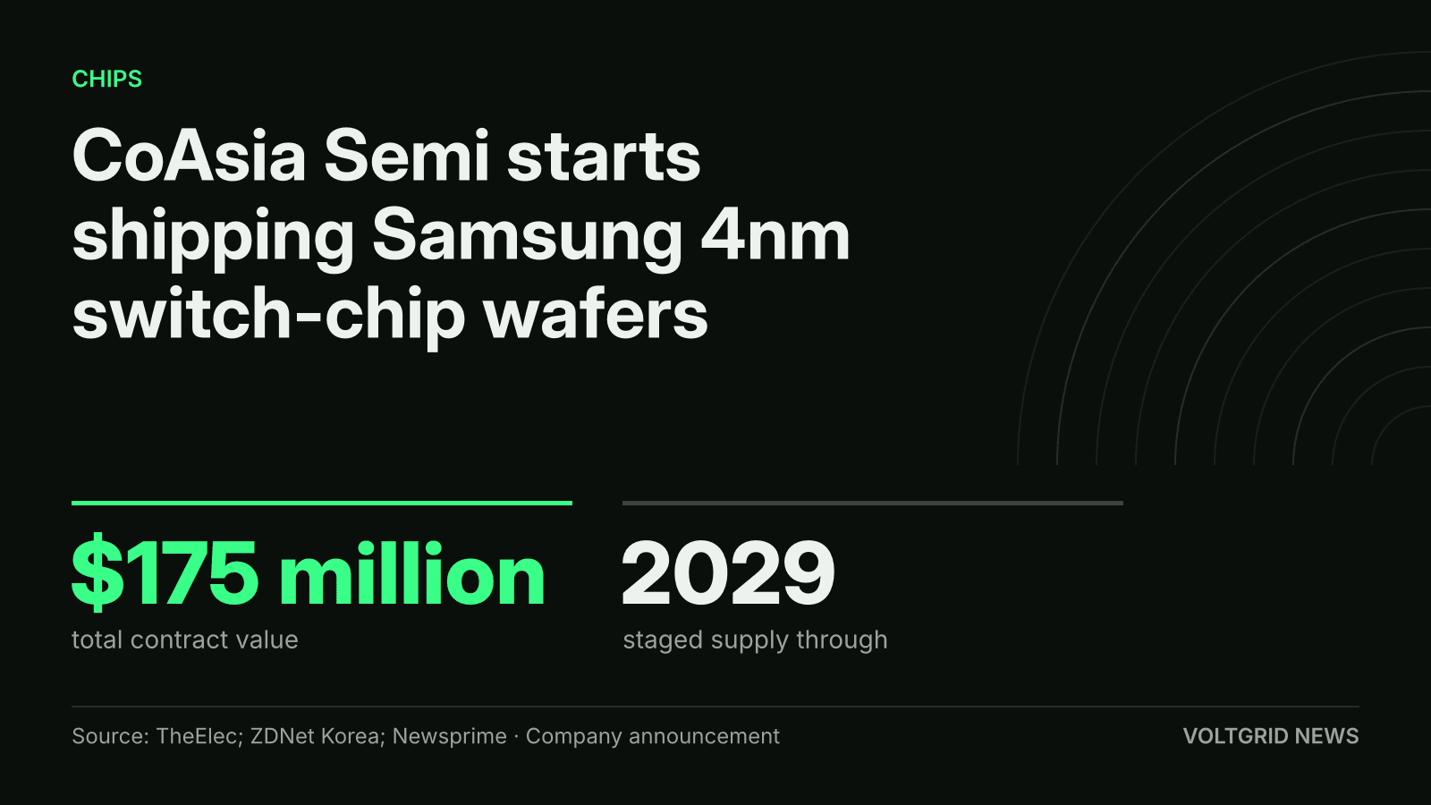
CoAsia Semi's Samsung 4nm switch-chip order is worth $175 million in total contract value, with staged supply through 2029, per TheElec.
Illustration (AI-generated)
CoAsia Semi, a South Korean semiconductor design house, said on Nov. 2 that it has begun mass-production shipments of wafers for network switch chips made on Samsung Electronics' 4nm foundry process, in a project worth $175 million through 2029, according to the company. The reports give the process as 4nm and name no Samsung variant (SF4, SF4P or SF4X).
The devices are network switch chips for high-performance computing (HPC), meaning high-speed data transmission and processing, according to The Elec and ZDNet Korea. Each die measures more than 800 square millimeters, which CoAsia Semi says is the largest chip it has handled in any project. Shipments began in mid-October.
The money is spread over time. The Elec reported that supplies will be delivered in stages through 2029 in line with the customer's production schedule, and that CoAsia Semi will recognize revenue as the wafers ship. ZDNet Korea and Newsprime put the $175 million at about 227 billion won, and Newsprime reports the work is done through CoAsia Semi, a subsidiary of listed CoAsia (045970). None of the reports names the end customer.
Why a Chip Above 800 mm² Is Hard to Make
A scanner prints a chip one exposure field at a time, and ASML specifies a maximum field of 26 x 33 mm for its NXE:3400C EUV system, so one die cannot grow past it. CoAsia Semi says its switch die is above 800 mm². For scale, NVIDIA's H100 GPU die measures 814 mm² on TSMC's 4N process, NVIDIA says.
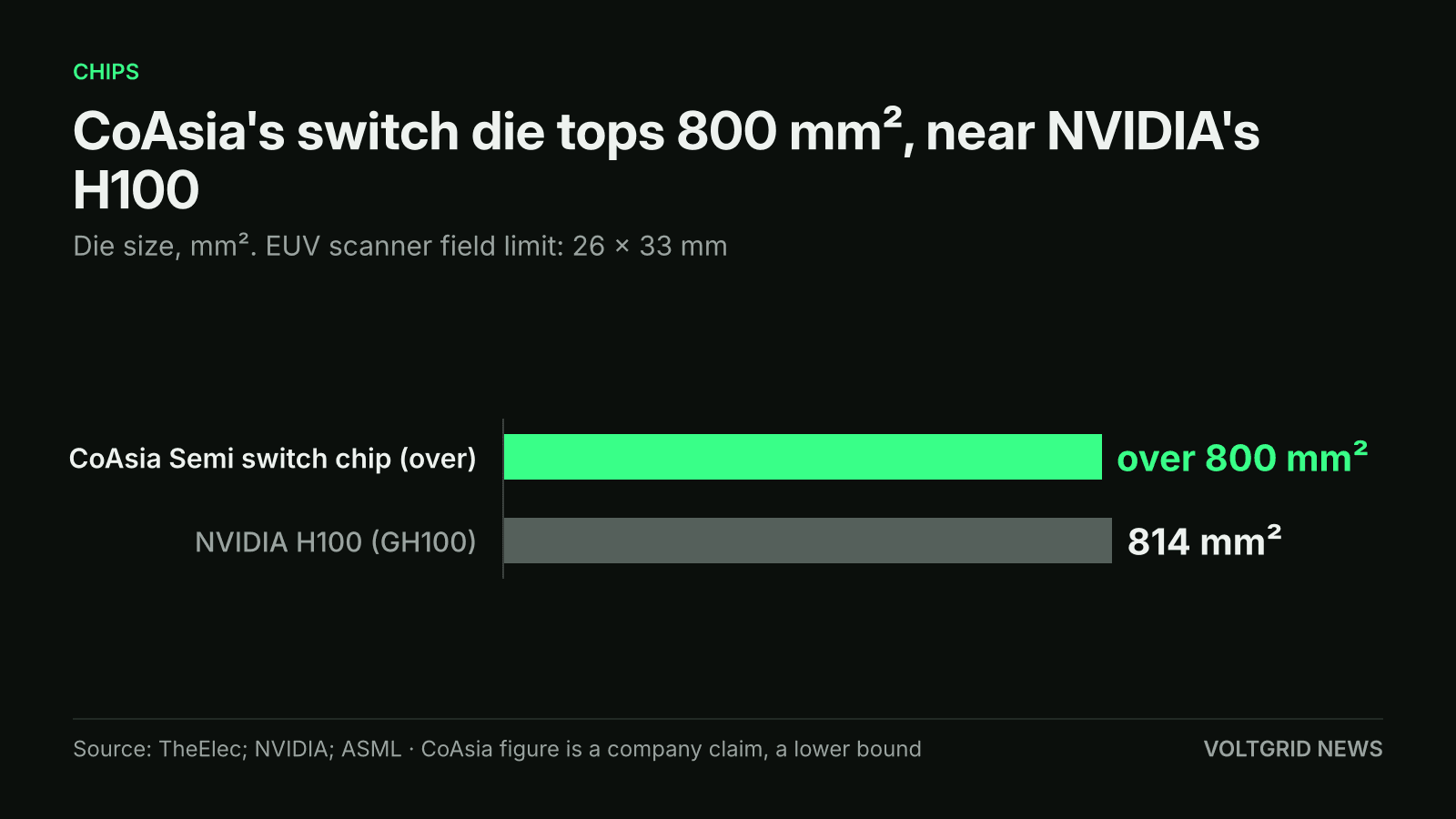
CoAsia Semi says its switch die is above 800 mm², close to the 814 mm² NVIDIA H100 die and bounded by the 26 x 33 mm EUV exposure field.
Illustration (AI-generated)
The Elec and ZDNet Korea both explain the difficulty in the same terms: the larger a die, the more likely a defect lands on it, which makes yield management harder, and power consumption and heat generation add design constraints. ZDNet Korea calls big-die production one of the highest technical barriers for a design house. CEO Shin Dong-soo said in the company's announcement, as reported by ZDNet Korea, that the value of design-service firms is shifting from design alone to the ability to finish mass production.
No report gives a yield, a power rating or a wafer count. For data-center readers that means the heat and power draw of these switch chips, a factor in rack design, is not yet public.
What it says about Samsung Foundry's 4nm line
A design house placing 4nm wafers in volume is useful evidence for Samsung Foundry, but the end customer is unnamed and the sources describe CoAsia Semi's announcement, not a Samsung statement. The Elec said CoAsia Semi secured the 4nm wafer capacity for this project in advance, amid intensifying competition for manufacturing capacity. The Elec reported earlier that Samsung is freeing 4nm capacity by moving its next modem to 2nm, with the room reportedly going to HBM base dies, so 4nm demand at Samsung now comes from more than one direction.
CoAsia Semi's other recent work, per The Elec: it has signed mass-production supply agreements for AI chiplets with Rebellions and Tenstorrent, and in August 2026 it became the first South Korean design house to begin mass production of an 8nm system-on-chip using three-dimensional integrated circuit (3D IC) packaging.
What is not confirmed yet
The customer, the switch chip's product name and the wafer volume are undisclosed, and the figures come from CoAsia Semi's own announcement. Neither report read by Voltgrid quotes Samsung Foundry or the customer. The company said it is working with the same customer on a follow-up project, but gave no scope or date.