Samsung Yokohama Packaging Lab to Add Glass Substrates, Wafer Bonding
Chairman Lee Jae-yong's Nov. 1 visit, his first since the Sept. 8 opening, came as Samsung said it will add wafer bonding and glass substrates; it gave no timetable.
Chips & Power DeskEdited by Ege Erten
2 min readAI-assisted
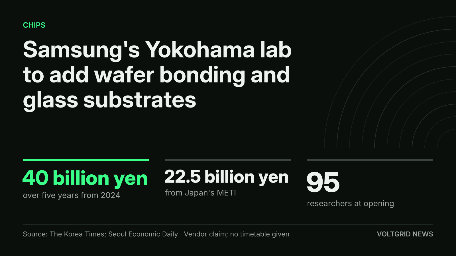
Samsung's Yokohama Advanced Package Lab runs on a 40 billion yen commitment over five years from 2024, with 22.5 billion yen from Japan's METI, Seoul Economic Daily reported.
Illustration (AI-generated)
Samsung Electronics Executive Chairman Lee Jae-yong toured the company's Yokohama packaging lab, the Advanced Package Lab (APL), on Nov. 1, and Samsung said the lab will widen its research to wafer bonding and glass substrates.
Samsung said Lee reviewed packaging materials and process work with researchers and discussed cooperation with Japan's materials, parts and equipment suppliers. According to The Korea Times, he pledged to keep expanding the research staff and to build the site into a global R&D hub for next-generation packaging. The visit was his first since the lab's formal opening on Sept. 8, Seoul Economic Daily reported.
Packaging is where HBM (high-bandwidth memory) stacks are joined to GPUs and accelerators in one package. It decides how fast data moves, how much power is spent moving it and how much heat the module must shed. That is why a lab in Yokohama matters to data-center buyers: HBM supply and rack power both depend on it.
Glass Substrates and Wafer Bonding Plans
The APL develops and validates materials and processes for advanced packaging. Samsung said it will extend that work to wafer bonding and glass substrates, and to new package structures for mass-produced, lower-power, high-performance chips, according to Seoul Economic Daily and The Korea Times.
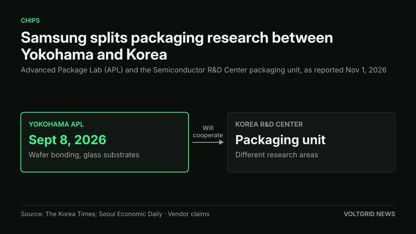
Samsung says the Yokohama lab's research areas differ from those of the packaging unit at its Korean R&D center, and the two will cooperate.
Illustration (AI-generated)
Samsung also said the lab's research areas will differ from those of the packaging team at its Semiconductor R&D Center in Korea, with the two units working together. Samsung said Japan was chosen for its dense cluster of materials and equipment makers and for government support of the semiconductor and AI industries.
The money is not new. Samsung has committed 40 billion yen, about $254 million according to The Korea Times, over five years from 2024. At the Sept. 8 opening, Seoul Economic Daily reported, Japan's trade ministry was to provide 22.5 billion yen of it, about 95 Korean and Japanese researchers were to work at the site, and 15 Japanese chip-related companies attended, among them Tokyo Electron and Ibiden.
Where it fits in the packaging race
Seoul Economic Daily describes TSMC as the global leader in advanced packaging and SK hynix as the leader in HBM, and says Samsung hopes to strengthen both through Japan. Samsung already works with more than 50 Japanese companies in AI-chip back-end processes, per the same report, which cites Nikkei. Local prototyping would let Samsung test new materials in Japan and move only promising ones to its Korean lines.
The visit follows other Samsung capacity moves that Voltgrid has tracked. Samsung is restarting a fifth Pyeongtaek fab to chase SK hynix in HBM and moving 4nm capacity to HBM base dies. Packaging supply is tight across the industry: NVIDIA said it plans 2.5 times more substrate capacity in three years, adding Samsung Electro-Mechanics as a supplier.
What is not confirmed yet
Samsung gave no timetable for glass substrates or wafer bonding, no headcount target beyond the opening-day figure, and no named customer or supplier agreement from the visit. No new spending was announced. The lab's output will show up, if at all, in how Samsung's HBM modules are packaged and qualified, which the company has not yet disclosed.
Sources
- 01Lee Jae-yong pushes Japan packaging hub to boost Samsung AI chip edgeGoogle News · AI chips · news.google.com
- 02Samsung Opens AI Chip Packaging Lab in Yokohama With Japanese State AidSeoul Economic Daily · en.sedaily.com
- 03Samsung chairman highlights chip packaging, visits Japanese unitThe Korea Times · koreatimes.co.kr
- 04Samsungs Jay Y. Lee Visits Japan Packaging Lab, Urges Tech PushSeoul Economic Daily · en.sedaily.com