Terafab Reportedly Targets 1M Wafers a Month by 2032, 700K Memory
Nikkei-sourced reports say Tesla and SpaceX's Terafab wants about 1M wafers a month, 700K for memory, near Samsung's DRAM capacity. Terafab has not confirmed it.
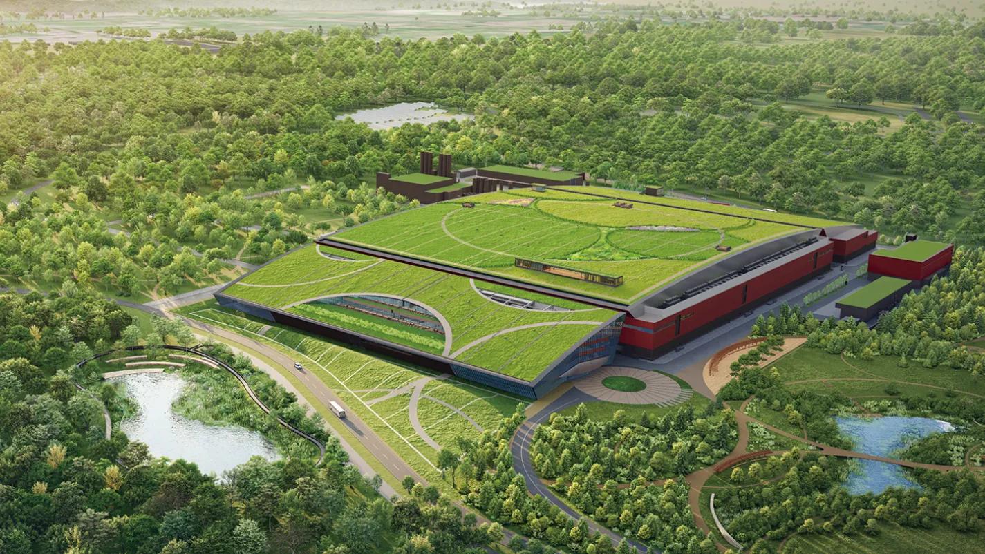
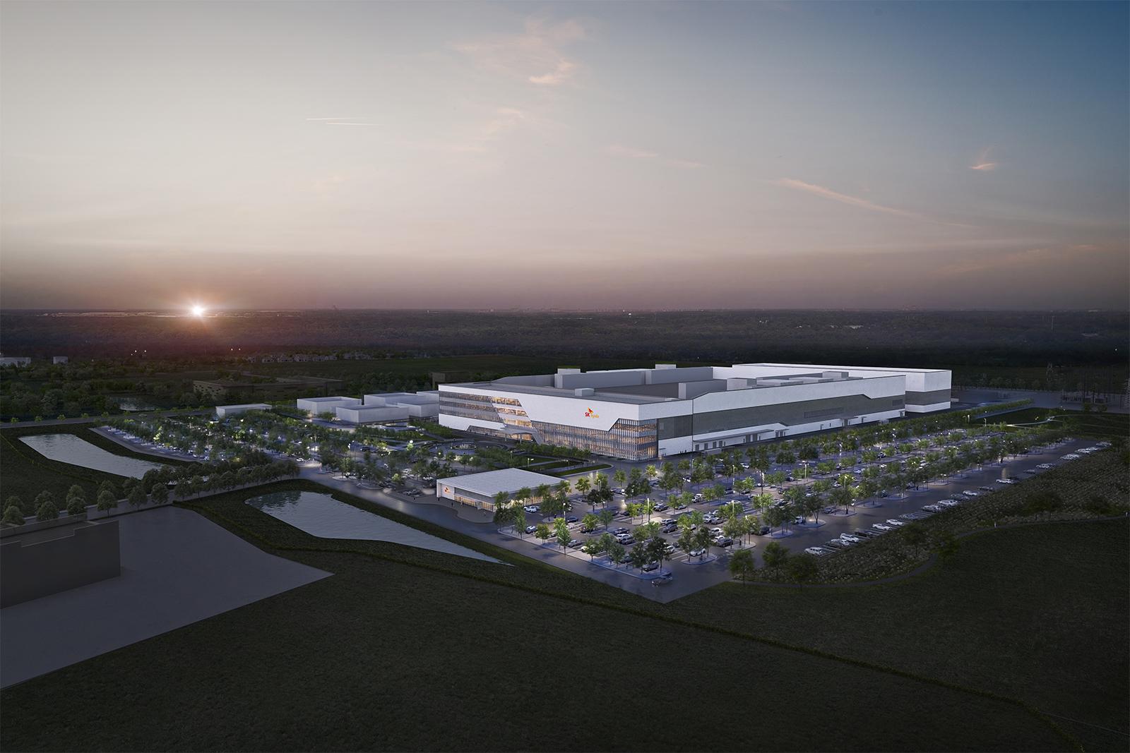
Rendering of Rapidus's IIM-1 plant in Chitose, Hokkaido. It does not show Terafab, which has no announced site.
Image: Rapidus
Source · Press image from the Rapidus website, used for news reporting.
Terafab, the Tesla and SpaceX chip project led by Elon Musk, has reportedly told equipment makers it wants about 1 million wafers a month after 2032, Nikkei reported on Nov. 9.
Terafab's reported memory capacity of 700,000 wafers a month matches the estimated size of Samsung's entire DRAM output; all figures are reported or estimated.
According to Nikkei, relayed by Financial News and TrendForce, the plan splits into roughly 700,000 wafers a month for memory chips and more than 300,000 for logic chips used in computing. Terafab reportedly gave the figures to toolmakers this autumn, and Nikkei says its procurement team made a confidential visit to Japan this month. Neither Terafab, Tesla nor SpaceX has confirmed the numbers.
Seoul Economic Daily, citing Nikkei, said the project aims to start mass production in the second half of 2028 and is placing orders with Japanese suppliers, some with delivery deadlines only months away. Industry officials told Nikkei it is unclear whether such a pace can be met.
Why the memory share matters
The reported 700,000 wafers a month for memory is about the size of Samsung Electronics' entire DRAM capacity, which is estimated at 650,000 to 700,000 wafers a month. For supply-chain watchers, that is the notable figure: a single newcomer would plan to match the world's largest DRAM maker in wafer starts, in a market where Samsung held 38% of Q3 DRAM revenue, as Voltgrid reported. It would also dwarf Japan's Rapidus, whose Chitose plant in Hokkaido is designed for 25,000 wafers a month, about one-fortieth of the reported Terafab total.
Wafer counts say nothing yet about output. TrendForce notes that Terafab has not disclosed how its memory capacity would be split between HBM (high-bandwidth memory) and LPDDR (low-power DRAM), or whether it would make and stack DRAM in-house or buy some chips for packaging.
Logic partners and the equipment race
For logic, Jiji Press reported that Terafab is leaning toward Intel's 2nm or 1.4nm processes, and TrendForce adds that Intel is reportedly coordinating technical support. TrendForce also says technical cooperation with Taiwanese companies on memory is under consideration, with no partner or arrangement confirmed.
The schedule is the hard part. Financial News notes that an advanced fab typically needs more than three years from construction planning to mass production, and that extra time is needed after tool installation to bring defect rates down. Terafab's earlier public target was volume output in Texas by the third quarter of 2028, which Musk set out on SpaceX's Q3 call; about 10 Korean suppliers were also reported to be in talks, with one firm tool commitment.
What is not confirmed yet
All figures here come from unnamed sources cited by Nikkei and its relayers. Terafab has published no wafer target, no memory split, no process partner and no equipment order list. Nikkei's phrasing of the date, "after 2032", differs from outlets that say "by 2032", so the year is itself unsettled. No fab site, power supply or capex figure for the 1 million wafer scale has been reported, so the electricity and cooling load of such a build cannot yet be estimated. Watch for tool-order disclosures from Japanese suppliers and any Terafab statement on the memory plan.