Micron G11 NAND Targets 400+ Layers, About 2x G9 Density, 2H27 Ramp
Micron's G11 NAND will exceed 400 layers with about 2x G9's bit density and ramp in 2H 2027; speed and energy gains are company claims, and Tom's Hardware's 42 Gb/mm2 and 5,400 MT/s figures are its own estimates.
3 min readAI-assisted
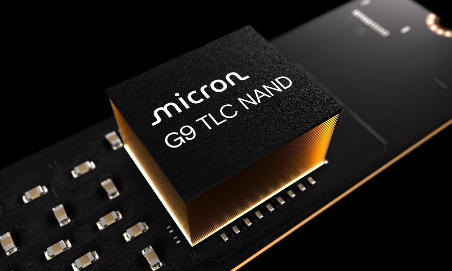
Micron's current G9 TLC NAND, the shipping 276-layer generation. This is G9, not G11: Micron has not released images of G11.
Image: Micron
Source · Press image from the Micron website, used for news reporting.
Micron said on Oct. 21 that its next-generation G11 NAND will have more than 400 layers and about twice the bit density of its current G9 generation, with volume ramp in the second half of 2027.

Micron says G11 will exceed 400 layers against 276 in G9; the exact G11 count is undisclosed, according to Blocks & Files and Tom's Hardware.
Illustration (AI-generated)
The company presented G11 at a technology and product webinar on its investor relations site, according to Blocks & Files. Scott DeBoer, Micron's president and chief technology and products officer, called it "the world's most advanced NAND" and said it skips the planned G10 generation. G9, which Micron is shipping, has 276 layers, according to Blocks & Files; Micron's own G9 page does not state the layer count.
Micron also claims up to 50% faster I/O than G9 and more than 25% lower energy to move each bit, according to Tom's Hardware; Blocks & Files words the energy gain as 25 percent less per bit. These are company claims. Tom's Hardware adds its own estimates of 42 Gb/mm2 and 5,400 MT/s, marked with question marks in its text, and Micron has not confirmed those numbers.
How Wafer Bonding Changes 3D NAND
In 3D NAND, memory cells are stacked in layers, and the circuits that read, write and move data normally sit beside or under that stack on the same wafer. Wafer-on-wafer bonding builds the memory array on one wafer and the peripheral logic and I/O on another, each with its own process, then joins the two. Micron has used logic under the array for several generations, Tom's Hardware notes, so bonding lets each part be tuned separately.
G11 will be the first Micron NAND to use wafer-on-wafer bonding. Tom's Hardware notes that Micron follows YMTC, which adopted the method earlier; Voltgrid reported this week that YMTC passed Samsung as China's top NAND supplier with a 38.5% share. DeBoer said the timing is right now that the technology is cost-effective and suits the product specifications.
Layers alone do not explain the density gain: Micron also cites an industry-leading cell pitch, which Tom's Hardware reads as smaller cells. Micron has not disclosed the number of active wordline layers or memory decks. It says it will give more detail in 2027, closer to launch.
Why G11 NAND Matters for AI Storage
Denser NAND means more terabytes in the same SSD footprint, which matters to operators who fill racks with flash next to accelerators. Lower energy per transferred bit, if it holds in shipping parts, trims the power that storage draws at fleet scale. Micron gave no watt figures for a drive, so the saving cannot yet be converted into rack power.
Blocks & Files reports that DeBoer also outlined two AI-oriented NAND directions. One is a high-IOPS SSD built on SLC-based small blocks, in the range of 25 million to 100 million IOPS, with next-generation drives that could hold up to 512 TB. The other is higher-bandwidth NAND with stacked dies connected by through-silicon vias, placed near the accelerator. DeBoer said that second path is costlier and would be built with customers.
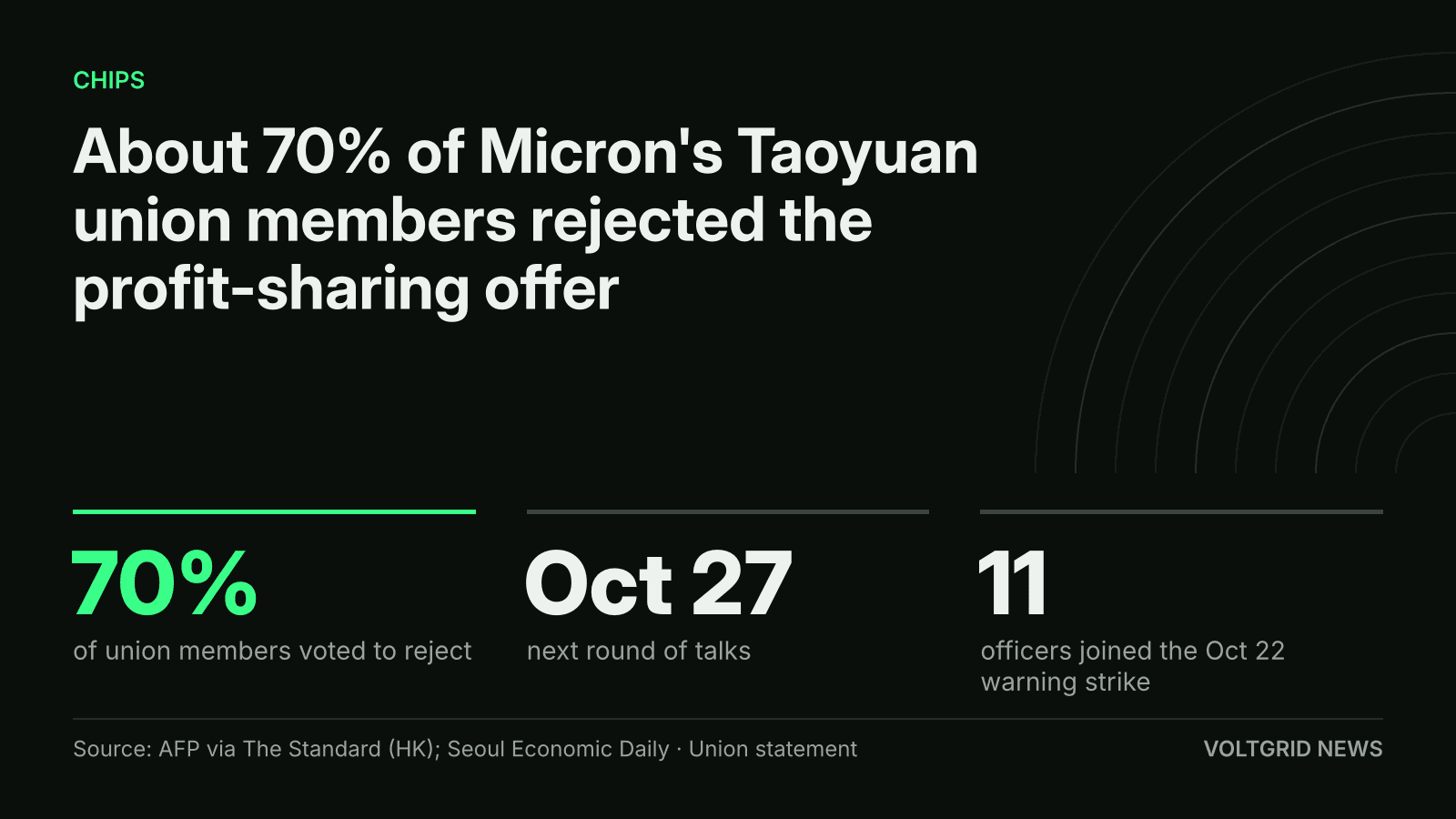
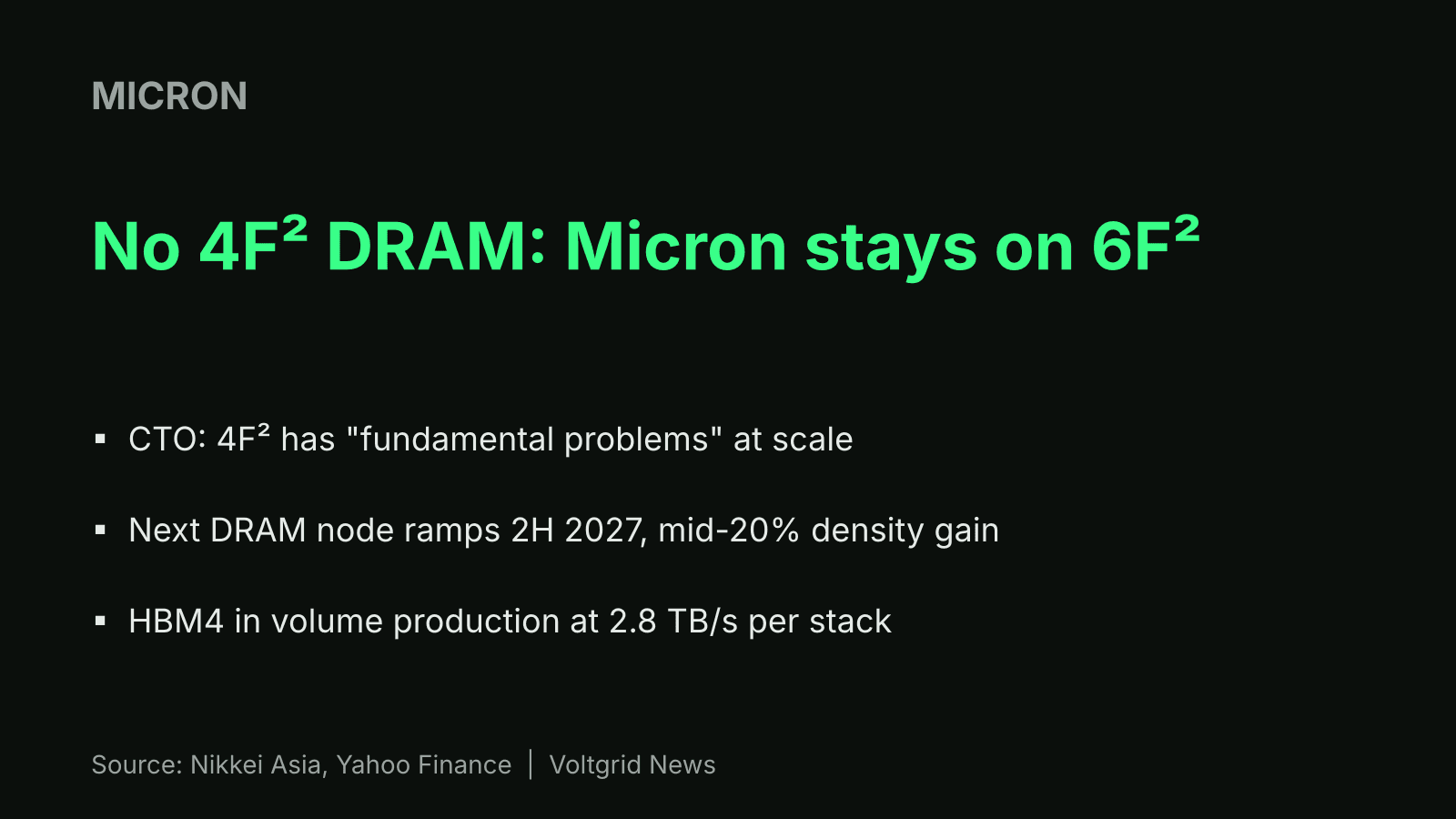
The webinar also covered DRAM and HBM, Blocks & Files reported; Voltgrid covered Micron's DRAM cell-layout choice on Oct. 21.
What Micron Has Not Confirmed About G11
Beyond relative gains, Micron has not published the exact layer count, the die density in Gb/mm2, the interface speed in MT/s or any product names for G11; it says only "more than 400" layers. The 2H 2027 ramp is a company target, and the performance and energy figures are Micron's own claims, not measured results. Watch for the 2027 technical disclosure and for the first SSD customers.