Samsung HBM Packaging Plant Breaks Ground; Lee Sees 40T Won ($30B) More
Reuters says President Lee Jae Myung put about 40 trillion won of equipment spending after Samsung's Asan HBM packaging fab; Seoul Economic Daily gives a mass-production target of May 2029.
Chips & Power DeskEdited by Ege Erten
3 min readAI-assisted
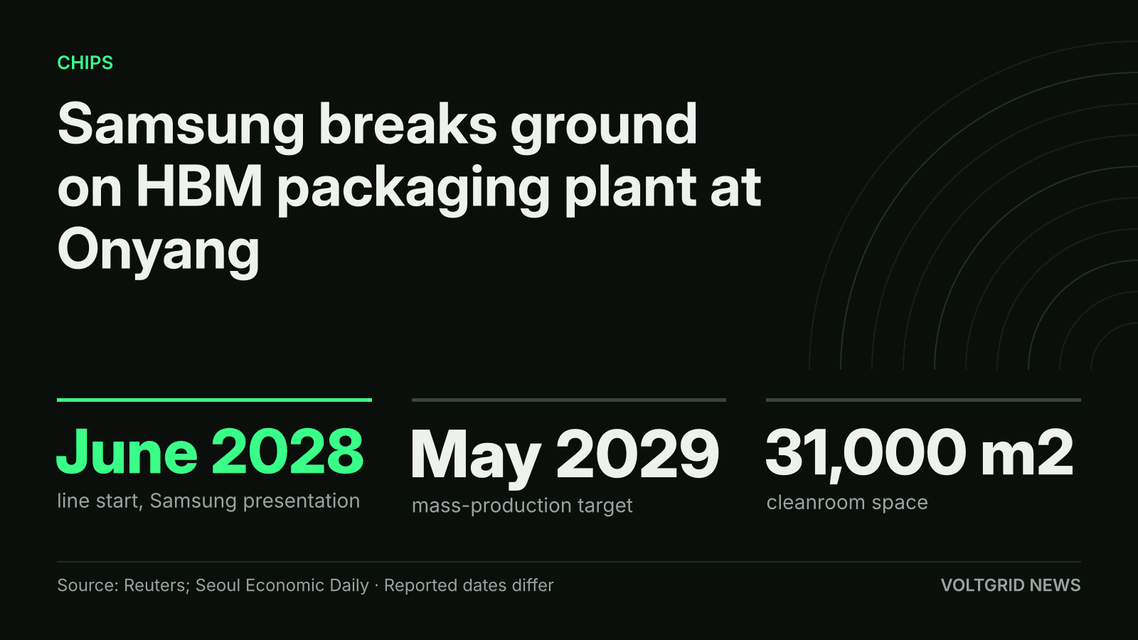
Reported dates for Samsung's Onyang HBM packaging plant differ between Reuters and Seoul Economic Daily.
Illustration (AI-generated)
South Korean President Lee Jae Myung said on Nov. 12 that Samsung Electronics' 6 trillion won ($4.48 billion) high-bandwidth memory (HBM) packaging plant in Asan will be followed by about 40 trillion won in investment in advanced equipment, according to Reuters. At the exchange rate Reuters used, 1,339.55 won to the dollar, the 40 trillion won comes to roughly $30 billion, the figure in Reuters' headline.
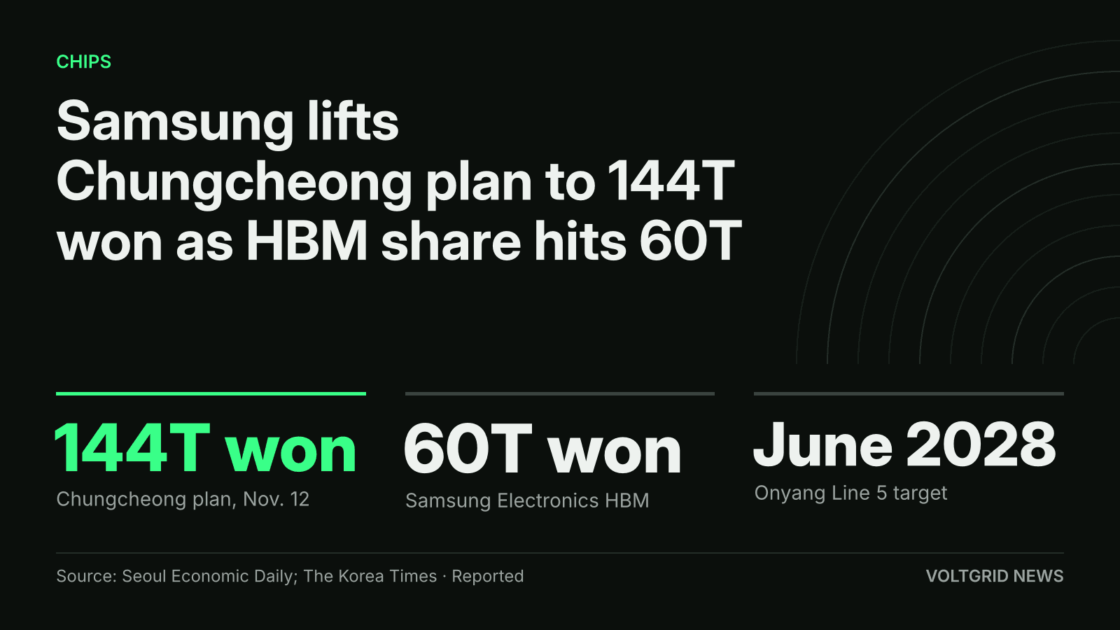
Lee spoke at a groundbreaking ceremony on Samsung's Onyang campus for part of the investment plans that Samsung affiliates announced in July, Reuters said. Samsung said in a presentation that the new HBM production line is scheduled to begin operating in June 2028, a year earlier than first planned, as it tries to meet fast-growing demand for server memory. Samsung also said the plant will have three floors of cleanroom space covering about 31,000 square metres.
Lee said about 40 trillion won of equipment spending will follow the 6 trillion won fab; Seoul Economic Daily gives 46 trillion won for Onyang.
Illustration (AI-generated)
The two figures Lee gave add up to 46 trillion won, which matches the total that Seoul Economic Daily says Samsung plans to invest at Onyang over the medium to long term to expand advanced packaging for HBM. Advanced packaging is the step that joins stacked memory dies into a module that sits beside an accelerator, so extra capacity there bears directly on how many HBM parts Samsung can ship. The company told investors on Oct. 29 that its 2027 HBM supply is sold out at target prices, as Voltgrid reported, which makes packaging output rather than demand the open question.
What the Onyang site adds
Seoul Economic Daily describes the new building as the Onyang No. 5 plant, dedicated to HBM advanced packaging. It reports that Samsung will spend about 1.3 trillion won ($900 million) on a 31,000-square-meter cleanroom, and that the campus floor area will grow from 270,000 to 420,000 square meters once the expansion is done. The paper adds that Samsung wants to extend packaging capacity that had been concentrated in Cheonan to Onyang.
Samsung Executive Chairman Jay Y. Lee said at the ceremony that Onyang, long a site for assembling and testing general-purpose chips, would become a base for HBM, the paper reported. He said Samsung would also pursue mega projects in the Honam and Yeongnam regions. The government has tapped Samsung, SK hynix and other companies for mega projects covering semiconductors, physical AI and AI data centers, Reuters said, and Seoul Economic Daily calls this the first of three such projects to break ground.
The move fits a pattern of packaging spending that Voltgrid has tracked. Samsung's chairman toured its Yokohama packaging lab on Nov. 1, when the company said it would add wafer bonding and glass substrates, as Voltgrid reported. Samsung gave no timetable for that work.
What is not confirmed yet
The sources disagree on the numbers for the plant itself. Reuters, citing a Samsung presentation, gives a 6 trillion won investment and a June 2028 start. Seoul Economic Daily gives about 1.3 trillion won for the Onyang No. 5 plant and a mass-production target of May 2029. Neither report explains the gap; the 1.3 trillion won may be one phase of the 6 trillion won, but that is our reading, not something either outlet states. The May 2029 date may also be the earlier schedule that Reuters says was brought forward.
Neither report gives HBM output, wafer or module capacity, customer names, or a schedule and split for the 40 trillion won of equipment spending, which Lee described as coming in stages. The $30 billion figure is Reuters' conversion of won, not a separate commitment from Samsung. We have not seen a Samsung statement or filing on the ceremony, only its presentation as described by Reuters.
Sources
- 01Lee Says Samsung's Onyang Campus to Become Key Hub for Advanced HBM PackagingSeoul Economic Daily · en.sedaily.com
- 02South Korea's Lee says Samsung chip packaging expansion to spur $30 billion additional investmentGoogle News · agenda, foundry and memory · news.google.com
- 03Samsung Breaks Ground on $900 Million HBM Packaging Plant in OnyangSeoul Economic Daily · en.sedaily.com